
Uncertainty, forecasting, and technology roadmaps the case of Moore’s Law
We have all spent the better part of this year obsessing over the shape and direction of infection curves. If there’s anything we’ve learned from our collective crash-course in epidemiology, it’s that the exercise of forecasting the future is quite hard. The models we’re building aren’t imbued with foresight no matter how complex (or, uh, simple) their underlying dynamics.
I will return to a more general discussion of forecasting and how institutional pressures influence the exercise at the end of this piece. I will first examine in more detail perhaps the most famous of contemporary forecasts: Moore’s Law. The simplified story is that we went from building-sized mainframes with lilliputian capabilities to carrying supercomputers in our pockets and it was made possible principally by the ongoing exponential increases in integration, a trend foreseen most elegantly by Gordon Moore in 1965. The apparent enduring accuracy of Moore’s projections has underpinned significant commentary about the technological possibilities of our future. I think in asking ourselves what the future holds we should examine more deeply what we’re using to predict the future.
This post will end up being lengthy so I’ll divide it into a few sections. First, I’ll explore in more detail the history and context in which Moore made his first forecast in 1965. Next, I’ll discuss how institutions evolved to extend and refresh Moore’s forecasts and orient the industry around his projections, ultimately creating a self-fulfilling prophecy. Lastly, I’ll discuss how those forecasts erred and finish with a broader discussion around the politics of forecasting. If you’re not interested in the history, skip to the final section. Given the importance of semiconductor technology to the last 40 years of technological progress and economic development, there is an already deep scholarship on the subject matter, which I’ll borrow from readily, but my intent is to explore not just how projections are shaped by and shape our actions but also examine the implications of inaccuracy and what that says about the nature of technological development.
Moore’s First Forecast
It’s worth beginning with some context for Moore’s original projection1. Today, the integrated circuit as the natural evolution of the transistor is taken as given. However, the future of semiconductor technology was far less certain in the early 1960s. Although transistors were evolving rapidly from the humble beginnings of Bell Labs’ point-contact transistor2, the industry faced significant reliability hurdles to large scale integration as circuits grew more complex. Jack Morton, Bell Labs’ VP, dubbed this the ‘tyranny of numbers’ and the industry, with significant support from the Department of Defense, was simultaneously developing a slew of technological approaches to addressing the problem in the early 1960s3. Different approaches included modular packaging (favored by Motorola and the Army), thin films and hybrid circuits (Corning, RCA, and the Navy), molecular electronics (Westinghouse and Air Force), and monolithic integrated circuits (invented by Noyce and Kilby at Fairchild and TI). As cited in Holbrook (see FN 3), only 25% of firms indicated they were pursuing monolithic (i.e. integrated circuits) approaches in a 1962 survey in Electronics Industries, by contrast both modular packaging and thin-film approaches had >50% support.
At the same time there was a chorus of voices claiming that the existing scientific paradigm of solid-state devices was ultimately a dead-end. As early as the late 1950s researchers began arguing that the ultimate fabrication limit of transistor devices was only an order of magnitude away. The same J.A. Morton from above drew on this line of thinking to advocate for a radically different approach to computing in place of increasingly complex integration: functional devices designed around new physical phenomena4. Although outside the scope of this discussion, there’s a fascinating history to this line of research5.
Nor was Gordon Moore the only technology executive who thought there was a bright future to integrated circuit technology. An IEEE Spectrum conference hosted in 1964 featured several prominent executives all arguing that integrated circuit production techniques (here, using the term broadly to encompass the various approaches discussed above) would offer advantages over discrete transistors in capability, yield and price.
Harry Knowles, a manager from Westinghouse’s Molecular Electronics Division wrote the following (emphasis mine),
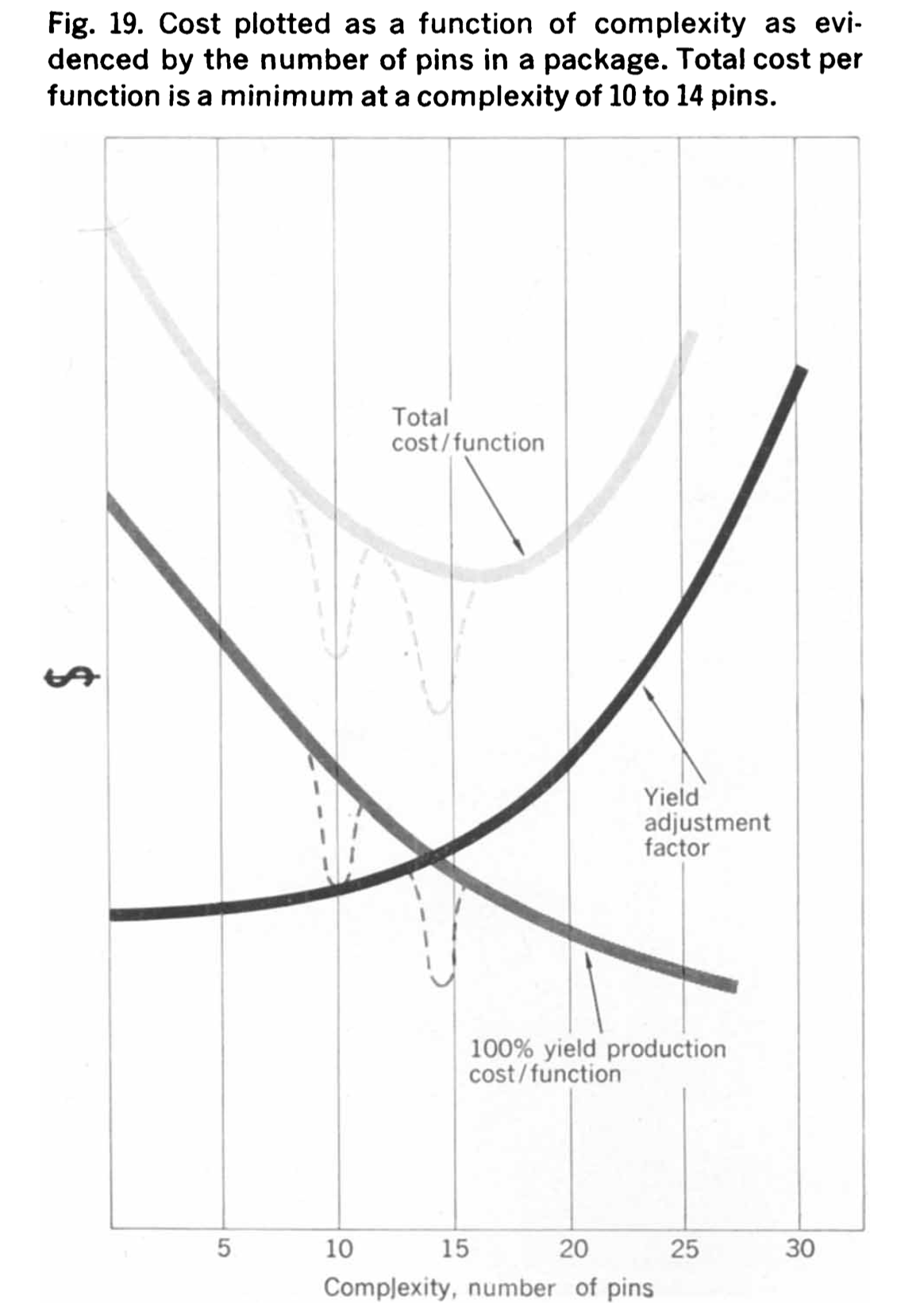
During 1964, a saturated logic time in the 10- nanosecond range will probably be achieved—and perhaps even a lower value. Speed has doubled every year over the past seven years on the average. Greater speeds depend upon mechanical tolerances. If transistors, diodes, resistors, etc., can be made smaller, the use of smaller parasitic capacitances implied thereby means that the speed of the circuits will be increased. … Masking tolerances are now in the 7- to 8-micron range, with a 15-ns saturated logic. We can soon expect 3- to 4-micron tolerances and 5- to 7-ns saturated logic. Electron-beam sensing and machining will permit 0.1- micron tolerances and subnanosecond logic speeds. Parenthetically, it is interesting to extrapolate on what a one-inch silicon slice would produce if the size of individual components were decreased by a factor of 15. Figure 22 shows an integrated circuit which may be fabricated on a silicon wafer at a density of about 800 gates per square inch, using 8-micron tolerances. If these tolerances were reduced to 0.5 micron, the area of the circuits would be reduced by slightly over 200. The number of circuits per square inch would then be about 16m000. In addition, the gates would operate 15 times faster or in the 1-ns delay range. Such a wafer would have a logic power about 100 times greater than today’s largest computer!
Knowles explicitly drew the link between continued miniaturization enabling higher performance (speed) and reliability and ultimately greater computing capacity. Knowles also included a graph that plotted the cost of an integrated circuit as a function of complexity6. Notably, yield drops precipitously as complexity increases, creating a U-shape with a sweet spot for price/# of pins at the frontier of current technological capabilities. Keep this graph in mind.
Moore published the first iteration of his eponymous Law in 1965 in Electronics magazine. Given the context above, I have always felt the best way to understand Moore’s 1965 piece is as an advertisement to technology executives about why they should choose integrated circuits 7. The readership of Electronics would include executives, technologists, and government officials who were trying to understand which technologies to bet on for future projects and Gordon Moore as the co-founder of Fairchild Semiconductor wanted to sell them integrated circuit technology.
There are a few choice hints to this motivation in the piece itself. Moore used language that would re-assure executives tasked with deciding what technology to build their newest offering with. He noted that “Integrated electronics is established today” and “[i]n almost every case, integrated electronics have demonstrated high reliability.” He then continued, “For most applications, semiconductor integrated circuits will predominate.” Moore’s message was clear: what seems like a risky bet on a novel technology is not actually one at all, you’re just the vanguard inventing the future.
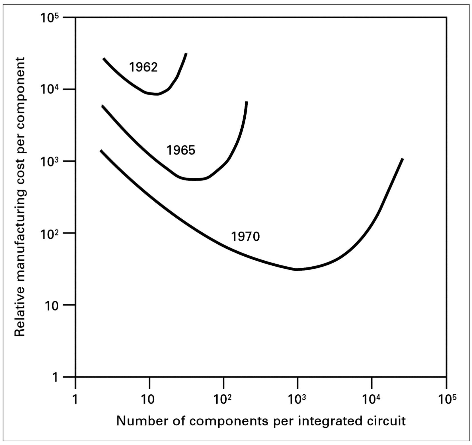
The marketing angle aside, the piece’s enduring legacy comes from Moore’s projections and his forecasts both built on the optimism of Knowles et al and directly responded to those in the community who felt the runway for the silicon integrated circuit paradigm was short. Moore extended Knowles’ analysis in a few ways. First, he presents the data in cost per component and total components per circuit. Second, and most importantly, he demonstrates how the curves might shift over the coming decade, showing a continual improvement in the cost/complexity minima. His extension illustrates the dynamic, evolving nature of the industry’s technological capabilities. If you’re a computing executive his message is that by the close of the decade you’ll be able to build an IC with 1000 components for the same price as one with 100 components in 1965 and this improvement in cost/function would make economical increasingly complex functions, growing the overall market of applications for ICs and computing.
Often overlooked with the relentless focus on semi-log plots as empirical proofs of Moore’s Law8, is that Moore explicitly disagreed with the industry’s doomsayers. Morton, of Bell Labs, also writing in 1965 warned sternly that “the frontiers of science had moved far away from electronics and no new promising physical phenomena loomed on the horizon that had obvious large-scale technological potential.” To Morton, the growing dissociation between science and electronics posed a threat to the industry’s future because “the speed or frequency response of germanium and silicon transistors is approaching the intrinsic limitation set by the materials and the fabrication methods based upon diffusion and visible light resolution techniques.” By contrast, Moore specifically argued that his projection for 65,000 components on a single wafer was possible with “present optical techniques” and that yields of 100% did not face thermodynamics limits or require “any fundamental research or to replace present processes.” Contra Morton’s call for returning to the well of science, Moore argued that “[o]nly the engineering effort is needed.” Again, for an executive, Moore was making the case that existing technologies and techniques were safe places to invest9.
Refreshing Forecasts and a Blueprint for the Future
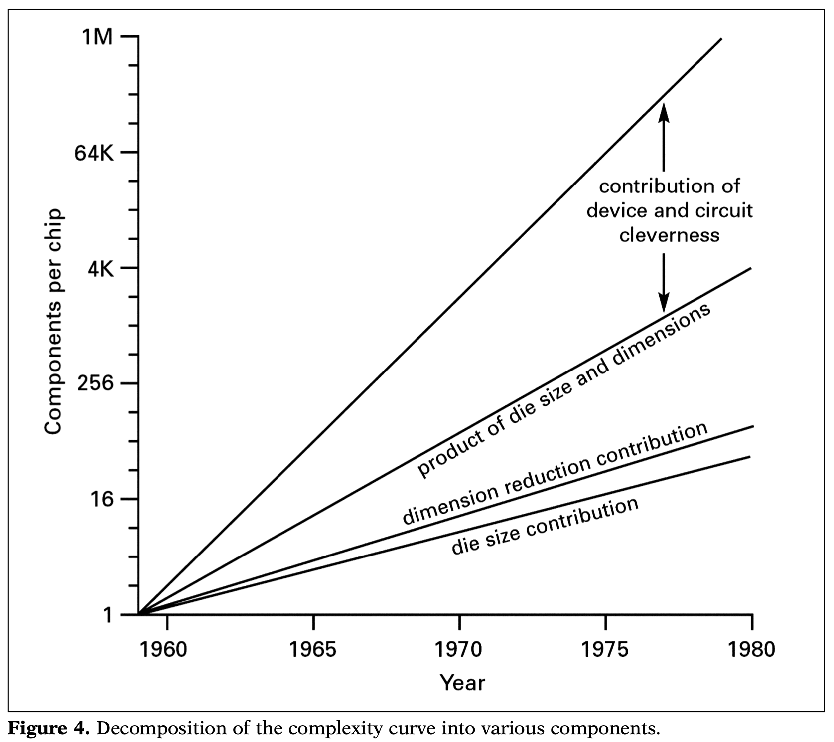
Moore published an updated projection on the future of integrated circuitry at the 1975 Electron Devices Meeting Conference. The paper was short and built directly on his 1965 piece. Moore extended the 1965 analysis by identifying three major drivers of the 64,000x increase in integration from 1965 through 1975: increasing die size (20x), decreasing transistor dimensions (32x), and increasing “circuit and device cleverness” (100x). Moore again argued that the first two faced no fundamental obstacles and should be expected to continue for the coming years, as long as it was economical. However, he felt that “circuit and device cleverness,” the largest driver of increased integration, would reach a peak with the introduction of Charge Coupled Devices and the overall trajectory of increasing integration would roughly half from doubling annually to doubling every two years. This is the version of Moore’s Law most commonly cited today.
Progress in the two drivers Moore predicted would continue, die size increases and transistor scaling, ultimately depended on advances in process technology. Another foundational paper published in the 1974 provided a blueprint for how designers could leverage advances in both doping (ion implantation) and lithography techniques for continued dimensional scaling of MOS integrated circuits into the sub micron regime. Dennard’s scaling (as it came to be called after the study’s lead author, Robert Dennard) is deceptively simple. In summary, scaling a transistor’s dimensions, voltages, and doping concentrations by the same factor allows designers to scale transistors to the sub-micron regime (see the table below from the original paper). Conveniently, this scaling approach mitigated concerns over heat dissipation because power density remained constant. That said, the authors also identified challenges that would arise from this approach, namely the lack of scaling in the sub-threshold voltage, which would become an issue in the early 2000s. Most importantly their paper demonstrated that by leveraging emerging process technologies sub-micron devices were physically realizable, not simply a theoretical abstraction.
To summarize: together these two papers provided a roadmap to sub-micron transistors and continued exponential increases in density. Make bigger chips with smaller transistors. To make smaller transistors leverage new process technologies to reduce the dimensions, voltages, and doping concentrations by the same factor.
Institutional responses to changing industry dynamics
The mid-1970s and early 1980s were a pivotal period in reshaping the industry’s institutional ecology. By this point, the industry had grown dramatically and monolithic integrated circuits, as invented by Kilby and Noyce, were an established technology within industry; government (read: defense) purchases were no longer the majority of IC sales by 1967 and less than a quarter of all semiconductor sales by 1968. The industry was also in the midst of a major technological shift from bipolar to MOS transistors, a technological shift that also upended the industry’s competitive dynamics10. According to data from ICE, MOS transistors, which were invented at Bell Labs in 1960, were 15% of all US semiconductor sales in 1970 but over 50% of sales by 1978, even as sales of bipolar ICs grew nearly 3x over the same period. New firms, best suited to take advantage of the technology, rose alongside MOS, to emerge as industry leaders. For example, Intel’s first successful product was the 1101 SRAM which had greater density and lower threshold voltages than competitors because of Intel’s innovation with the silicon-gate process 11.
However, the questions raised in the previous decade about the ultimate limits to silicon transistor technology remained an open area of research and motivated considerable investment by industry labs and government agencies in alternatives to silicon ICs. IBM researchers argued in 1969 that “based on extrapolation of present technology” limits to speed were only an order of magnitude away and thus “[p]rogress beyond this point can only be made by radical deviations from the current lines of development” 12. Research labs cited exactly these types of concerns in their papers outlining novel technologies like IBM’s superconducting Josephon-Junctions or TI’s research program into quantum-effects devices (with support from DARPA)13. The Office of Naval Research also began an ambitious program in the 1970s investigating “ultra sub-micron” devices that aimed to develop technology with 20 Angstrom feature sizes, roughly half the size of modern leading edge transistors. In addition to research in novel devices, these programs helped to accelerate discoveries in the sub-nano scale and usher in the dawn of nanotechnology writ large 14.
Lastly, the 1980s re-shaped the industry’s competitive dynamics. After several decades of American dominance, the 1980s brought significant upheaval as Japanese manufacturers captured a majority of industry market share due to their dominance in DRAM, which was then the single largest submarket in integrated circuits 15. Crucially, the emergence of Japan’s semiconductor and computing industries was significantly aided by government programs orchestrated by Japan’s Ministry of International Trade and Industry (MITI)16.
American semiconductor manufacturers responded to their loss of dominance by creating new institutions aimed squarely at improving competitiveness with international competition. The first such institution was the Semiconductor Industry Association (SIA, 1977) founded to lobby for protection from purported Japanese dumping. Five years later in 1982, industry executives formed the Semiconductor Research Corporation (SRC) as a collaborative industry venture to fund academic research in silicon integrated circuits. The SRC’s first annual report specifically mentioned the divergence of DoD research priorities, which focused primarily on non-silicon materials systems such as GaAs, from industry needs and international competition as motivations for the creation of the SRC 17. Funding for the SRC was only $5M in its first year and has remained modest relative to industry R&D funding throughout its existence18. The last notable institution founded in the 1980s was SEMATECH19. SEMATECH, jointly funded by DoD, was originally intended to be a horizontal collaboration between manufacturers on advanced process technology. Instead, the consortium pivoted to focus on vertical collaboration between suppliers and manufacturers.
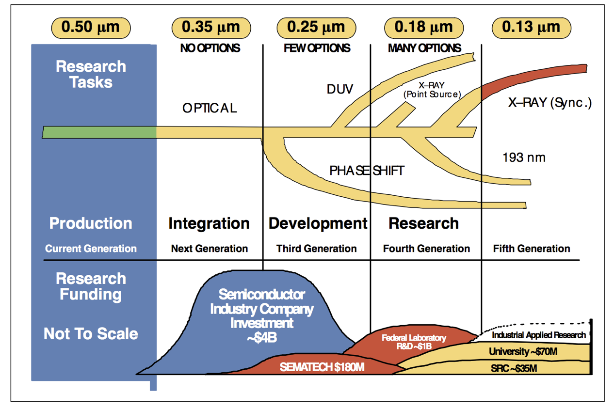
One other major change took place in the industry’s institutional structure: the hollowing out of central research laboratories. As the industry’s competitive dynamics changed due to the emergence of international competition and the rise of fabless design firms, centralized research labs became an expensive and increasingly hard to justify relic. The research labs that conducted long-range work in alternatives to CMOS saw their budgets cut as firms focused R&D closer to production. The result was a division of research labor across institutions and organizations as described in the below chart from the 1994 National Technology Roadmap for Semiconductors (NTRS). Given the intensity of competition in process development, ~75% of semiconductor research was conducted by industry and highly concentrated on the next process node. As you moved further out from production research fell into the domain of a different set of specialized institutions. Federal Labs and SEMATECH were 2-3 nodes from production and the SRC and universities were 3+ nodes from production. In addition to the vastly different funding scales between industry and consortia, it’s important to note R&D conducted outside industry served to vet potential options for future production that got refined by firms in the run-up to commercialization.
Institutionalizing Moore’s Law
Look closely at the graphic above, explicit is the notion that that the cadence of Moore’s Law would continue for several more nodes (transistors scale by 0.7x each generation) and the industry’s division of research labor was organized around that assumption. It is worth taking a step back, again to the 1980s, to explore how this assumption became embedded in the industry’s institutional structure before we discuss the consequences.
Collaborative research consortia in the US and Japan during the 70s/80s were a major catalyst for the codification of industry-wide technology roadmaps. In coming together to agree on a research agenda for collaborative consortia, competitors sketched out an agreed upon vision for the future of the industry’s technology and what it would take to get there. In the US, this process was driven most acutely by the SRC whose 1984 SRC summer research conference published 10-year goals to help researchers identify areas of need for the industry. Government agencies also asked for industry guidance on where to spend their research dollars. The White House OSTP organized a conference of industry, government, and academic researchers “to identify the most critical efforts that should be undertaken to develop the [0.12 micron] manufacturing process” by the year 200020. The first government coordinated roadmap, Micro Tech 2000, was deemed overly aggressive and eventually the exercise fell to the industry’s trade association, the SIA, to coordinate.
The first edition of the SIA’s National Technology Roadmap for Semiconductors (NTRS) was published in 1992 and coordinated by the SIA’s newly created “Technology Committee,” originally chaired by Gordon Moore. As alluded to in the name the 1992 NTRS was a US based exercise, as were the 1994 and 1997 refreshes. Each edition of the roadmap was a 15-year projection for the industry’s largest product categories (DRAMs and CPUs). In 1998 the roadmap committee admitted international members from Japan and Europe’s semiconductor associations21.
From 1998 through 2015 the roadmap was fully refreshed every other year. Therefore, the NTRS/ITRS roadmap archive is a rich dataset for evaluating expert consensus on the future of the semiconductor industry at regular intervals. Below, I plot NTRS/ITRS projections from 1992 through 2001 for the same variables that Moore plotted in his 1975 paper alongside actual data from Stanford’s CPU DB22.
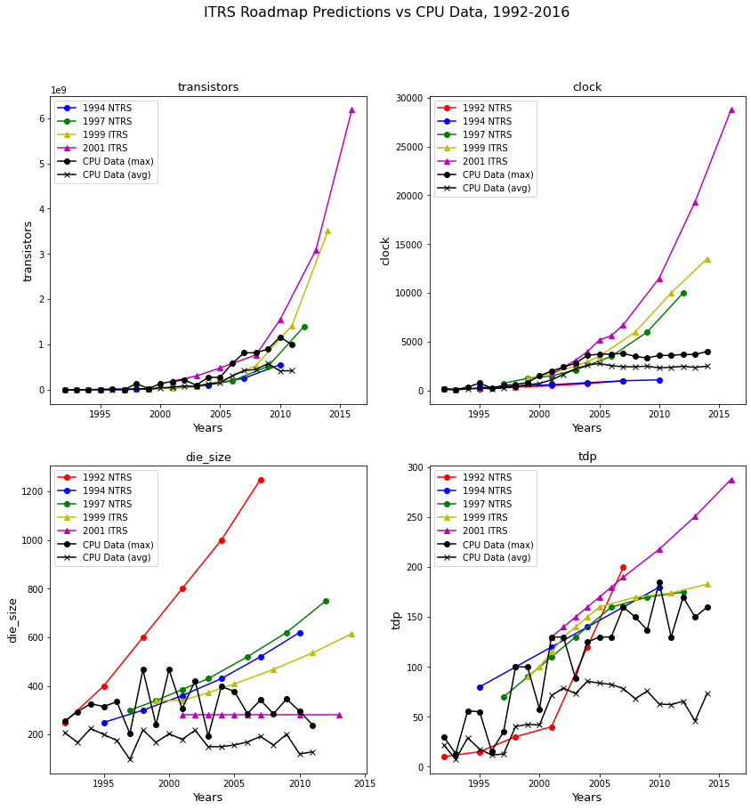
To my eye, two primary themes emerge from these charts: 1. The multi-faceted nature of technological progress 2. The contingent and path dependent nature of technological forecasts
Technological Progress comes in many forms
Moore’s 1975 paper disaggregated increasing integration into three main drivers: die size increases, transistor size reductions, circuit cleverness. The chart above shows that initial projections anticipated a continuation of both die size increases and transistor size reductions but only the latter kept pace with projections. However, overall transistor counts continued to scale exponentially through the early 2010s (when my dataset ends).
Engineers compensated for limitations in die size by scaling transistor size faster than projected trends. Ultimately, the industry began facing other technical limitations to its pursuit of aggressive scaling. By the late 90s, leakage currents began to be a significant source of power draw as gate oxide thicknesses were reduced to nearly a single monolayer. From roughly 2000 onwards the industry began introducing both new materials and transistor geometries to offset these issues and continue scaling. The introduction of high-K metal gates, strained silicon, air gaps, and FinFETs all increased process complexity and drove up costs but ultimately allowed the continued pursuit of transistor miniaturization (albeit with worsening economics)23.
There’s another key point to raise from the graph above however: unanticipated limits to progress. In 2003 the industry hit a major inflection point as CPU designs began hitting thermal limits. You can see this most acutely in the divergence of projected clock speeds from realized clock speeds. As late as the 2003 roadmap the industry was projecting 20GHz CPU speeds in 2020! Instead, today’s latest CPUs have base frequencies around 3GHz and top out at 5GHz in bursts. The story here is simple: the roadmap assumed ever increasing TDPs but in practice systems were capped at about 200W TDP. The graph below shows the clustering beginning in the early 2000s as designers hit that wall. Although the industry responded by shifting to multi-core processors, the real world user benefits from that transition were not automatic and required software designers capable enough of fully utilizing the capabilities of those CPUs24. The fact that it wasn’t widely anticipated also meant the wider ecosystem was unprepared to take advantage of multi-core processors.
The contingent and path dependent nature of technological progress
As I said in the introduction, we’ve spent a lot of time this year discussing various pandemic forecasts and separate from the pandemic there are plenty of examples of expert forecasts being consistently and frustratingly off-base (EIA’s solar forecasts are the ones that are most top of mind). The reason I’m so interested in the performance of NTRS/ITRS roadmaps is because they show cleanly how poorly institutions anticipate deviations from a prevailing trajectory.
The roadmaps were borne out of the assumption that Moore’s Law would continue unabated and be driven by the same levers and as reality diverged (e.g. die size limits) the industry compensated by accelerating transistor size reduction to maintain the integration trajectory. However, even that approach hit hard limits and the roadmaps again failed to anticipate those. Paolo Gargini, formerly of Intel, told me that when the roadmaps went international a majority of metrics had changes to their projections as non-US based scientists and firms provided input. When we talk about the endurance of Moore’s Law the story is about how the industry maintained Moore’s Law, which itself is shaped by who was in the room in crafting the roadmap. Technologies aren’t autonomous but rather the result of community effort.
Our technological capabilities are of course bound by the laws of nature and limits of our scientific knowledge but ultimately what we achieve is primarily a function of the effort directed toward a particular vision. Given enough funding, enough brainpower, and enough dedication humans have proven quite adept at bringing into reality what had previously existed only in the mind’s eye.
As detailed above, the US institutional context was shaped by the military, AT&T, IBM, and Japanese competition. The collaborative institutions were all dominated by IDMs (SIA, SRC, SEMATECH, NTRS/ITRS). For these firms, market leadership in the semiconductor industry went hand-in-hand with manufacturing leadership and this was reflected in the research agendas of those institutions. There was a massive international collaboration on the transistion to larger wafers (first 300mm then 450mm, which sputtered out) to drive down manufacturing costs. Similarly, the industry’s largest manufacturers took equity ownership of the only EUV manufacturer, ASML, during the development of EUV technology. The industry’s technological collaboration focused on manufacturing technology.
Moore’s Law Forever?
This brings me to my ultimate point: in a technological ecosystem as rich in opportunity as computing, firms will invest dollars where their marginal impact is highest. For decades, the success of the Moore’s Law trajectory led to a natural division of labor. Integrated manufacturers invested heavily in capex to accelerate transistor reduction and could capture returns from a few core products (CPUs, DRAMs, GPUs) that were leveraged by the entire ecosystem. The year-over-year improvements in those chips was sufficient to limit the scope of exploration by other firms. If you were a programmer or system designer, you were happy to take the extra computing power via Moore’s Law and use it wastefully.
As Moore’s Law has slowed the most effective use of a marginal dollar has moved up the stack. Firms began to realize this shift early in the 2010s and we’ve seen a slate of announcements in that vain: Google’s TPUs and Apple’s M1 chips signal a shift back to vertical integration. System designers are now saying the tight coupling of chip design with system design is worth paying the non-recurring engineering (NRE) costs of designing a new chip. While the headlines all say “Moore’s Law has ended,” I think the point to focus on is we’re on the precipice of a new S-curve as firms explore technological levers that previously were ignored while the WinTel duopoly was at its heights. In fact, it may be possible that we see several distinct curves as firms find varying levels of success. Some solution areas may be more amenable to existing techniques (e.g. the success of GPUs in machine learning) while others may require still un-discovered science. For this reason, semiconductors may go from a general-purpose technology to one where progress is more dispersed across application areas. All of this precludes the commercialization of entirely new computing elements25 or the possibilities of something like quantum computing.
The future of computing is likely to be more exciting than the last two decades where we all ended up with smartphones and laptops that looked and behaved very similarly. I predict we’ll see more experimentation as folks test what’s possible now that old assumptions have died. Breakthroughs still on the horizon may in fact pan out. While that future seems secure, it is worth further reflection on the lessons for policy makers and industry executives. We predicted Moore’s Law would continue and then one day it stopped. Why weren’t we backtesting our assumptions? Why weren’t our institutions prepared for that transition? The irony of our current predicament is US firms have now undoubtedly lost their manufacturing lead. I’ll write separately about the policy lessons to take from 40 years of public-private partnership that resulted in loss of technological leadership despite gearing our science apparatus around that singular goal.
-
My abridged discussion will borrow heavily from some of my own unpublished work and “Understanding Moore’s Law” by David Brock, which I recommend as further reading. ↩
-
A few recommended reads: ↩
-
Holbrook, 1995 ↩
-
Early pieces on impending limits: J.A. Morton: From Physics to Function, 1965 ↩
-
Alternatives to silicon ICs ↩
-
Chapter 3 of Understanding Moore’s Law gives more history on miniaturization in the computing and semiconductor history. ↩
-
Moore uses the term “integrated electronics” which he defines to include, “microassembly techniques for individual components, thin-film structures and semiconductor integrated circuits.” ↩
-
Compare Moore’s projection to Knowles’ from the year prior. Moore’s forecast of 65,000 components on a circuit is about two years beyond what Knowles cited as possible in the excerpt above. Ultimately, they were both extrapolating from the same limited data. ↩
-
One consideration when evaluating the different perspectives of these two men is that Moore was an entrepreneur and Morton an executive at the world’s premier industrial research lab; they were both talking their book, in a sense. ↩
-
Highly recommend reading Ross Knox Bassett’s book if you’re interested in the emergence of MOS ↩
-
Keyes, 1969. Physical problems and limits in computer logic. IEEE Spectrum. ↩
-
Hungsub Choi and Cyrus C. M. Mody, “The Long History of Molecular Electronics: Microelectronics Origins of Nanotechnology, “SocialStudies of Science. For details on TI’s program see Bate, R.T., 1986. “The future of microstructure technology — The industry view,” which specifically references work from TI’s device group foreseeing limits to MOS around 0.5 micron (Chatterjee et al. 1983, “Modeling of small MOS devices and device limits”). ↩
-
cite Mody’s book ↩
-
cite data on Japan’s rise ↩
-
First SRC Annual Report ↩
-
Much has been written about SEMATECH and its impact on the industry so I’ll focus my discussion on the overall institutional structure. Good papers include: ↩
-
NACS 1991 ↩
-
Paolo Gargini has a nice presentation detailing the history of industry and the roadmap and the changes that occurred as it internationalized. I do not have permission to share it broadly but can with interested folks. ↩
-
CPU DB cite. Unfortunately their data ends by 2012 but its sufficient for the purposes of this post. Maybe if I have the energy I’ll update it with more recent data. ↩
-
Nvidia Moore’s Law over ↩
-
Neil Thompson cite ↩
-
alternatives to CMOS ↩